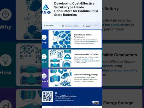
Imagine a world powered by an endless supply of clean, safe, and affordable energy. As the global demand for electric vehicles and renewable grid storage skyrockets, traditional lithium-ion batteries are reaching their physical and economic limits. Enter Dr. Ananya Banik and her pioneering research team in Chemistry and Chemical Biology, who are spearheading a major breakthrough in next-generation energy storage.
A Game-Changing Shift from Lithium to Sodium
For years, lithium has dominated the battery industry. However, supply chain constraints and high extraction costs make scaling up lithium-ion technology increasingly difficult. Sodium, on the other hand, is abundant, eco-friendly, and significantly cheaper to source.
By shifting the focus toward sodium-based chemistries, researchers are opening up brand-new possibilities for sustainable power. This initiative represents a massive leap forward in solid state battery development, proving that high-performance energy storage can be both accessible and cost-effective.
Overcoming Roadblocks in Solid State Technology
While conventional batteries rely on liquid electrolytes—which can leak or pose severe fire risks—solid-state designs replace liquids with solid materials. This crucial upgrade dramatically improves safety, extends lifespan, and boosts energy density.
Supported by forward-thinking initiatives like ANRF PRISM, recent solid state battery development focuses on solving key stability and performance challenges. Dr. Banik’s team is refining solid sodium electrolytes to ensure that high conductivity and structural stability can coexist without driving up production costs.
What This Means for the Global Energy Transition
The impact of affordable sodium solid-state batteries extends far beyond the laboratory. Lowering battery production costs will directly accelerate the adoption of electric vehicles and make large-scale solar and wind energy storage feasible for developing economies.
As solid state battery development continues to gain momentum, innovations like these bring us one step closer to a cleaner, self-reliant, and fully electrified future for everyone.